MOORE’S LAW
June 10, 2016
There is absolutely no doubt the invention and development of chip technology has changed the world and made possible a remarkable number of devices we seemingly cannot live without. It has also made possible miniaturization of electronics considered impossible thirty years ago. This post is about the rapid improvement that technology and those of you who read my posts are probably very familiar with Moor’s Law. Let us restate and refresh our memories.
“Moore’s law” is the observation that, over the history of computing hardware, the number of transistors in a dense integrated circuit has doubled approximately every two years.”
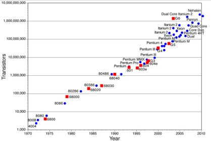
You can see from the digital above, that law is represented in graph form with the actual “chip” designation given. Most people will be familiar with Moore’s Law, which was not so much a law, but a prediction given by Intel’s Gordon Moore. His theory was stated in 1965. Currently, the density of components on a silicon wafer is close to reaching its physical limit but there are promising technologies that should supersede transistors to overcome this “shaky” fact. Just who is Dr. Gordon Moore?
GORDON E. MOORE:
Gordon Earle Moore was born January 3, 1929. He is an American businessman, co-founder and Chairman Emeritus of Intel Corporation, and the author of Moore’s law. Moore was born in San Francisco, California, and grew up in nearby Pescadero. He attended Sequoia High School in Redwood City and initially went to San Jose State University. After two years he transferred to the University of California, Berkeley, from which he received a Bachelor of Science degree in chemistry in 1950.
In September, 1950 Moore matriculated at the California Institute of Technology (Caltech), where he received a PhD in chemistry and a minor in physics, all awarded in 1954. Moore conducted postdoctoral research at the Applied Physics Laboratory at Johns Hopkins University from 1953 to 1956.
Moore joined MIT and Caltech alumnus William Shockley at the Shockley Semiconductor Laboratory division of Beckman Instruments, but left with the “traitorous eight“, when Sherman Fairchild agreed to fund their efforts to created the influential Fairchild Semiconductor corporation.
In July 1968, Robert Noyce and Moore founded NM Electronics which later became Intel Corporation where he served as Executive Vice President until 1975. He then became President. In April 1979, Moore became Chairman of the Board and Chief Executive Officer, holding that position until April 1987, when he became Chairman of the Board. He was named Chairman Emeritus of Intel Corporation in 1997. Under Noyce, Moore, and later Andrew Grove, Intel has pioneered new technologies in the areas of computer memory, integrated circuits and microprocessor design. A picture of Dr. Moore is given as follows:

JUST HOW DO YOU MAKE A COMPUTER CHIP?
We are going to use Intel as our example although there are several “chip” manufacturers in the world. The top ten (10) are as follows:
- INTEL = $48.7 billion in sales
- Samsung = $28.6 billion in sales
- Texas Instruments = $14 billion in sales.
- Toshiba = $12.7 billion in sales
- Renesas = $ 10.6 billion in sales
- Qualcomm = $10.2 billion in sales
- ST Microelectronics = $ 9.7 billion in sales
- Hynix = $9.3 billion in sales
- Micron = $7.4 billion in sales
- Broadcom = $7.2 billion in sales
As you can see, INTEL is by far the biggest, producing the greatest number of computer chips.
The deserts of Arizona are home to Intel’s Fab 32, a $3 billion factory that is performing one of the most complicated electrical engineering feats of our time. It’s here that processors with components measuring just forty-five (45) millionths of a millimeter across are manufactured, ready to be shipped to motherboard manufacturers all over the world. Creating these complicated miniature systems is impressive enough, but it’s not the processors’ diminutive size that’s the most startling or impressive part of the process. It may seem an impossible transformation, but these fiendishly complex components are made from nothing more glamorous than sand. Such a transformative feat isn’t simple. The production process requires more than three hundred (300) individual steps.
STEP ONE:
Sand is composed of silica (also known as silicon dioxide), and is the starting point for making a processor. Sand used in the building industry is often yellow, orange or red due to impurities, but the type chosen in the manufacture of silicon is a much purer form known as silica sand, which is usually recovered by quarrying. To extract the element silicon from the silica, it must be reduced (in other words, have the oxygen removed from it). This is accomplished by heating a mixture of silica and carbon in an electric arc furnace to a temperature in excess of 2,000°C. The carbon reacts with the oxygen in the molten silica to produce carbon dioxide (a by-product) and silicon, which settles in the bottom of the furnace. The remaining silicon is then treated with oxygen to reduce any calcium and aluminum impurities. The end result of this process is a substance referred to as metallurgical-grade silicon, which is up to ninety-nine percent (99 %) pure.
This is not nearly pure enough for semiconductor manufacture, however, so the next job is to refine the metallurgical-grade silicon further. The silicon is ground to a fine powder and reacted with gaseous hydrogen chloride in a fluidized bed reactor at 300°C giving a liquid compound of silicon called trichlorosilane.
Impurities such as iron, aluminum, boron and phosphorous also react to give their chlorides, which are then removed by fractional distillation. The purified trichlorosilane is vaporized and reacted with hydrogen gas at 1,100°C so that the elemental silicon is retrieved.
During the reaction, silicon is deposited on the surface of an electrically heated ultra-pure silicon rod to produce a silicon ingot. The end result is referred to as electronic-grade silicon, and has a purity of 99.999999 per cent. (Incredible purity.)
STEP TWO:
Although pure to a very high degree, raw electronic-grade silicon has a polycrystalline structure. In other words, it’s made of many small silicon crystals, with defects called grain boundaries. Because these anomalies affect local electronic behavior, polycrystalline silicon is unsuitable for semiconductor manufacturing. To turn it into a usable material, the silicon must be transformed into single crystals that have a regular atomic structure. This transformation is achieved through the Czochralski Process. Electronic-grade silicon is melted in a rotating quartz crucible and held at just above its melting point of 1,414°C. A tiny crystal of silicon is then dipped into the molten silicon and slowly withdrawn while being continuously rotated in the opposite direction to the rotation of the crucible. The crystal acts as a seed, causing silicon from the crucible to crystallize around it. This builds up a rod – called a boule – that comprises a single silicon crystal. The diameter of the boule depends on the temperature in the crucible, the rate at which the crystal is ‘pulled’ (which is measured in millimeters per hour) and the speed of rotation. A typical boule measures 300mm in diameter.
STEP THREE:
Integrated circuits are approximately linear, which is to say that they’re formed on the surface of the silicon. To maximize the surface area of silicon available for making chips, the boule is sliced up into discs called wafers. The wafers are just thick enough to allow them to be handled safely during semiconductor fabrication. 300mm wafers are typically 0.775mm thick. Sawing is carried out using a wire saw that cuts multiple slices simultaneously, in the same way that some kitchen gadgets cut an egg into several slices in a single operation.
Silicon saws differ from kitchen tools in that the wire is constantly moving and carries with it a slurry of silicon carbide, the same abrasive material that forms the surface of ‘wet-dry’ sandpaper. The sharp edges of each wafer are then smoothed to prevent the wafers from chipping during later processes.
Next, in a procedure called ‘lapping’, the surfaces are polished using an abrasive slurry until the wafers are flat to within an astonishing 2μm (two thousandths of a millimeter). The wafer is then etched in a mixture of nitric, hydrofluoric and acetic acids. The nitric acid oxides the surfaces to give a thin layer of silicon dioxide – which the hydrofluoric acid immediately dissolves away to leave a clean silicon surface – and the acetic acid controls the reaction rate. The result of all this refining and treating is an even smoother and cleaner surface.
STEP FOUR:
In many of the subsequent steps, the electrical properties of the wafer will be modified through exposure to ion beams, hot gasses and chemicals. But this needs to be done selectively to specific areas of the wafer in order to build up the circuit. A multistage process is used to create an oxide layer in the shape of the required circuit features. In some cases, this procedure can be achieved using ‘photoresist’, a photosensitive chemical not dissimilar to that used in making photographic film (just as described in steps B, C and D, below).
Where hot gasses are involved, however, the photoresist would be destroyed, making another, more complicated method of masking the wafer necessary. To overcome the problem, a patterned oxide layer is applied to the wafer so that the hot gasses only reach the silicon in those areas where the oxide layer is missing. Applying the oxide layer mask to the wafer is a multistage process, as illustrated as follows.
(A) The wafer is heated to a high temperature in a furnace. The surface layer of silicon reacts with the oxygen present to create a layer of silicon dioxide.
(B) A layer of photoresist is applied. The wafer is spun in a vacuum so that the photoresist spreads out evenly over the surface before being baked dry.
(C) The wafer is exposed to ultraviolet light through a photographic mask or film. This mask defines the required pattern of circuit features. This process has to be carried out many times, once for each chip or rectangular cluster of chips on the wafer. The film is moved between each exposure using a machine called a ‘stepper’.
(D) The next stage is to develop the latent circuit image. This process is carried out using an alkaline solution. During this process, those parts of the photoresist that were exposed to the ultraviolet soften in the solution and are washed away.
(E) The photoresist isn’t sufficiently durable to withstand the hot gasses used in some steps, but it is able to withstand hydrofluoric acid, which is now used to dissolve those parts of the silicon oxide layer where the photoresist has been washed away.
(F) Finally, a solvent is used to remove the remaining photoresist, leaving a patterned oxide layer in the shape of the required circuit features.
STEP FIVE:
The fundamental building block of a processor is a type of transistor called a MOSFET. There are “P” channels and “N” channels. The first step in creating a circuit is to create n-type and p-type regions. Below is given the method Intel uses for its 90nm process and beyond:
(A) The wafer is exposed to a beam of boron ions. These implant themselves into the silicon through the gaps in a layer of photoresist to create areas called ‘p-wells’. These are, confusingly enough, used in the n-channel MOSFETs.
A boron ion is a boron atom that has had an electron removed, thereby giving it a positive charge. This charge allows the ions to be accelerated electrostatically in much the same way that electrons are accelerated towards the front of a CRT television, giving them enough energy to become implanted into the silicon.
(B) A different photoresist pattern is now applied, and a beam of phosphorous ions is used in the same way to create ‘n-wells’ for the p-channel MOSFETs.
(C) In the final ion implantation stage, following the application of yet another photoresist, another beam of phosphorous ions is used to create the n-type regions in the p-wells that will act as the source and drain of the n-channel MOSFETs. This has to be carried out separately from the creation of the n-wells because it needs a greater concentration of phosphorous ions to create n-type regions in p-type silicon than it takes to create n-type regions in pure, un-doped silicon.
(D) Next, following the deposition of a patterned oxide layer (because, once again, the photoresist would be destroyed by the hot gas used here), a layer of silicon-germanium doped with boron (which is a p-type material) is applied.
That’s just about it. I know this is long and torturous but we did say there were approximately three hundred steps in producing a chip.
OVERALL SUMMARY:
The way a chip works is the result of how a chip’s transistors and gates are designed and the ultimate use of the chip. Design specifications that include chip size, number of transistors, testing, and production factors are used to create schematics—symbolic representations of the transistors and interconnections that control the flow of electricity though a chip.
Designers then make stencil-like patterns, called masks, of each layer. Designers use computer-aided design (CAD) workstations to perform comprehensive simulations and tests of the chip functions. To design, test, and fine-tune a chip and make it ready for fabrication takes hundreds of people.
The “recipe” for making a chip varies depending on the chip’s proposed use. Making chips is a complex process requiring hundreds of precisely controlled steps that result in patterned layers of various materials built one on top of another.
A photolithographic “printing” process is used to form a chip’s multilayered transistors and interconnects (electrical circuits) on a wafer. Hundreds of identical processors are created in batches on a single silicon wafer. A JPEG of an INTEL wafer is given as follows:

Once all the layers are completed, a computer performs a process called wafer sort test. The testing ensures that the chips perform to design specifications.
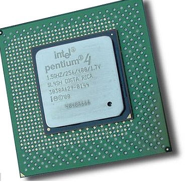
After fabrication, it’s time for packaging. The wafer is cut into individual pieces called die. The die is packaged between a substrate and a heat spreader to form a completed processor. The package protects the die and delivers critical power and electrical connections when placed directly into a computer circuit board or mobile device, such as a smartphone or tablet. The chip below is an INTEL Pentium 4 version.
Intel makes chips that have many different applications and use a variety of packaging technologies. Intel packages undergo final testing for functionality, performance, and power. Chips are electrically coded, visually inspected, and packaged in protective shipping material for shipment to Intel customers and retail.
CONCLUSIONS:
Genius is a wonderful thing and Dr. Gordon E. Moore was certainly a genius. I think their celebrity is never celebrated enough. We know the entertainment “stars”, sports “stars”, political “want-to-bees” get their press coverage but nine out of ten individuals do not know those who have contributed significantly to better lives for us. People such as Dr. Moore. Today is the funeral of Caius Clay; AKA Muhammad Ali. A great boxer and we are told a really kind man. I have no doubt both are true. His funeral has been televised and on-going for about four (4) hours now. Do you think Dr. Moore will get the recognition Mr. Ali is getting when he dies? Just a thought.


February 1, 2018 at 15:51
Great post. Whom should I ask for permission to use the photo of the wafer in an article? It’s the second from last photo.
LikeLike
April 27, 2017 at 18:29
Really great post, I certainly adore this site, keep on it.
LikeLike
May 16, 2017 at 07:00
Hello Mike. Thank you so much for taking a look at my post. As you well know, it’s not for everyone because most people choose other blogs to read. Mine is mostly technical in nature. Again, many thanks. Bob
LikeLike